mpw-005 — SKY130 MPW-5 reticle 5CS8011AC
- Foundry product
- EF MPW#5 (+ 'With ReRAM' split lot)
- Reticle set
- 5CS8011AC
- Run date
- 2022-03-21
- Submissions closed
- 2022-03-21
- Projects
- 74
- Fab lot
- 4229389
- Identification
- confirmed — Lot records: EF MPW#5, lot 4229389 = 'SKY130 MPW 5'
- Shuttle page
- archived copy of https://platform.efabless.com/shuttles/MPW-5 — the platform that hosted it is gone
- Foundry data
- third_party/shuttle/sky130/mpw-005/foundry
42 mask layers rendered
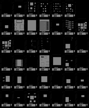
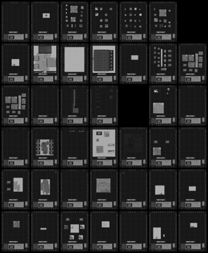
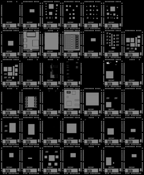
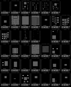
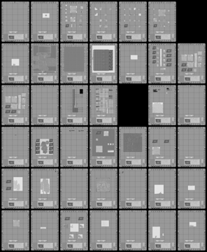
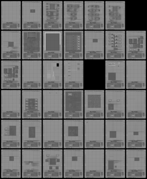
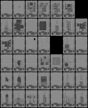
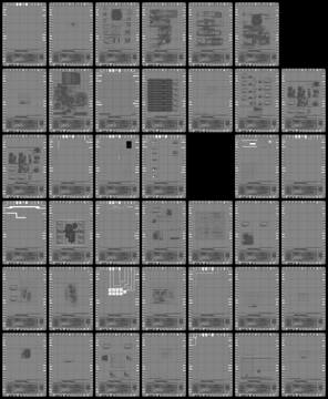
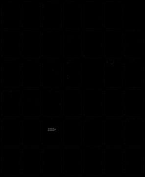
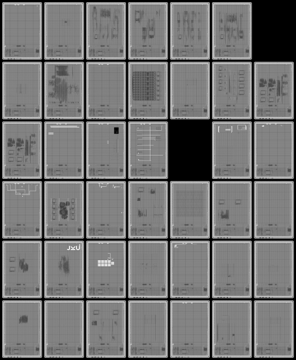
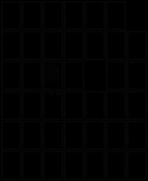
In process order — the order the wafer meets them, by the step number in the second column; the 6 layers with no step number are listed last. Each thumbnail is the whole reticle: all 40 dies stitched at their manifest frame positions.
| Mask | Process step | Layers | Dies with shapes | Shapes | |
|---|---|---|---|---|---|
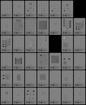 |
FOM
Field Oxide FOM = diff OR tap (OR grown pnp emitter) |
4 Field oxide mask |
drawn 65:20, 65:44 fill 23:28 on mask GDS 23:0 |
40 of 40 | 82,403,356 |
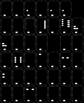 |
DNM
Deep N-Well DNM = dnwell sized by cdnm.3 |
7 Deep N-well mask |
drawn 64:18 on mask GDS 48:0 |
40 of 40 | 20,309 |
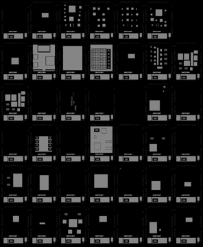 |
LVTNM
Low Vt Nch* drawn lvtn plus a created part [nwell AND (hvtp OR areaid.ce)] OR (LV nwell over varactors); only the drawn part is rendered |
14 Low Vt NOMOS mask |
drawn 125:44 on mask GDS 25:0 derived 125:44 OR (64:20 AND (78:44 OR 81:2)) |
40 of 40 | 132,148 |
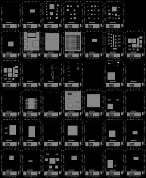 |
NWM
N-Well* NWM = nwell sized (cnwm.3a outside hvi / 3b inside), with DEPMOS/pwell-resistor exemptions |
17 N-well mask |
drawn 64:20 on mask GDS 21:0 |
40 of 40 | 26,260,556 |
 |
HVTPM
High Vt PCh* created over (LV nwell = nwell NOT hvi) NOT lvtn, plus hvtp only where nwell overlaps a varactor; the fab algorithm says do NOT OR hvtp in. Rendered as nwell = a superset |
22 High V P-channel implant mask |
drawn 64:20 on mask GDS 97:0 derived (64:20 NOT 75:20) NOT 125:44 |
40 of 40 | 104,428 |
 |
PWBM
P-Well Block Mask not used in SKY130 |
26 P-well block mask |
drawn 19:44 | 0 of 40 unused on this shuttle |
0 |
 |
PWDEM
P-Well Drain Extended pwde drawing not used in SKY130 |
30 P-well drain extended mask |
drawn 124:20 | 0 of 40 unused on this shuttle |
0 |
 |
TUNM
Tunnel Mask TUNM = tunm sized by ctunm.3 |
35 Tunnel mask |
drawn 80:20 on mask GDS 20:0 |
1 of 40 | 16 |
 |
ONOM
ONO Mask ONOM = tunm sized by clonom.3 (conom 87:44 is the fab's precomputed layer, not drawn) |
41 ONO mask |
drawn 80:20 on mask GDS 88:0 |
1 of 40 | 16 |
 |
LVOM
Low Voltage Oxide LVOM = hvi OR tunm and the SKY130 layer sheet |
44 Low voltage oxide mask |
drawn 75:20, 80:20 on mask GDS 46:0 |
40 of 40 | 1,996,759 |
 |
RPM
Resistor Protect |
49 Resistor protect mask |
drawn 86:20 on mask GDS 96:0 |
4 of 40 | 179 |
 |
URPM
Ultra-high resistor poly mask |
55 Ultra-high resistor poly mask |
drawn 79:20 | 40 of 40 | 119 |
 |
P1M
Poly 1 |
61 Poly mask |
drawn 66:20 fill 28:28 on mask GDS 28:0 |
40 of 40 | 213,238,980 |
 |
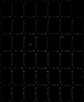
NTM
N-tip Implant created over nwell, ldntm and hvi (outside areaid.ce; rpm too in some flows) (cntm 26:20 is the fab's precomputed layer, not drawn) |
64 NTM mask(tip fomation) |
drawn 64:20, 75:20, 11:44 on mask GDS 27:0 derived 64:20 OR 11:44 OR (75:20 NOT 81:2) |
40 of 40 | 110,972 |
 |
HVNTM
High Volt. N-tip drawn hvntm merged with a created part (ndiff AND hvi, outside areaid.ce); only the drawn part is rendered |
68 HV N-tip mask formation |
drawn 125:20 on mask GDS 39:0 derived 125:20 OR ((65:20 AND 93:44 AND 75:20) NOT 81:2) |
40 of 40 | 549,793 |
 |
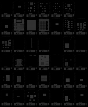
LDNTM
Lightly Doped N-tip |
71 LD tip layer mask |
drawn 11:44 on mask GDS 11:0 |
1 of 40 | 42 |
 |
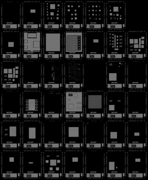
NPCM
Nitride Poly Cut |
78 Nitride poly cut mask |
drawn 95:20 on mask GDS 49:0 |
40 of 40 | 20,166,002 |
 |
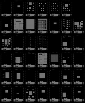
PSDM
P+ Implant PSDM = psdm OR grown psdm over pnp emitters |
81 P+ source drain implant mask |
drawn 94:20 on mask GDS 32:0 |
40 of 40 | 31,537,227 |
 |
PSDI
PSDI second P+ implant, same drawn layer as PSDM |
82 PSDI |
drawn 94:20 | 40 of 40 | 31,537,227 |
 |
NSDM
N+ Implant |
85 N+ source drain implant mask |
drawn 93:44 on mask GDS 30:0 |
40 of 40 | 36,320,822 |
 |
LICM1
Local Intr Cont.1 LICM1 = licon1 sized (clicm1.3a/3b by spacing) Via 0 (???→M0) |
93 Local interconnect contact mask |
drawn 66:44 on mask GDS 43:0 |
40 of 40 | 397,442,461 |
 |
LI1M
Local Intrcnct 1 LI (Metal 0) |
102 Local interconnect 1 mask |
drawn 67:20 fill 56:28 on mask GDS 56:0 |
40 of 40 | 203,765,710 |
 |
CTM1
Contact CTM1 = mcon (li1->met1) Via 1 (LI/M0→M1) |
107 Metal contact mask |
drawn 67:44 on mask GDS 35:0 |
40 of 40 | 361,238,161 |
 |
MM1
Metal 1 Metal 1 |
113 Metal1 mask |
drawn 68:20 fill 36:28 on mask GDS 36:0 |
40 of 40 | 667,890,484 |
 |
VIM
Via in the sky130B RRAM tier this is cviam, the lower half of the split via1; the upper half is VIMC (r1v) Via 1 (M1→M2) |
118 Via1 mask |
drawn 68:44 on mask GDS 40:0 |
40 of 40 | 67,190,811 |
 |
MM2
Metal 2 Metal 2 |
124 Metal mask2 |
drawn 69:20 fill 41:28 on mask GDS 41:0 |
40 of 40 | 523,692,389 |
 |
VIM2
Via 2-PLM Via 2 (M2→M3) variants: Via 2-TNV, Via 2-S8TM, Via 2-PLM |
129 Via2 mask |
drawn 69:44 on mask GDS 44:0 |
40 of 40 | 33,560,413 |
 |
CAPM
Capacitor MiM not used in SKY130 |
137 Capacitor mask |
drawn 89:44 | 40 of 40 | 5,384 |
 |
MM3
Metal 3-PLM Metal 3 variants: Metal 3-TLM, Metal 3-S8TM, Metal 3-PLM |
139 Metal3 mask |
drawn 70:20 fill 34:28 on mask GDS 34:0 |
40 of 40 | 198,625,512 |
 |
VIM3
Via3-PLM Via 3 (M3→M4) |
144 Via3 mask |
drawn 70:44 on mask GDS 50:0 |
40 of 40 | 34,408,584 |
 |
CAP2M
Capacitor mask |
152 Capacitor mask |
drawn 97:44 | 40 of 40 | 1,751 |
 |
MM4
Metal 4 Metal 4 |
154 Metal mask4 |
drawn 71:20 fill 51:28 on mask GDS 51:0 |
40 of 40 | 201,505,342 |
 |
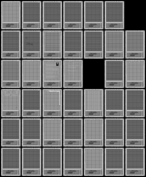
VIM4
Via4 Via 4 (M4→M5) |
159 Via pad mask |
drawn 71:44 on mask GDS 58:0 |
40 of 40 | 9,759,787 |
 |
MM5
Metal 5 Metal 5 |
162 Metal5 mask |
drawn 72:20 fill 59:28 on mask GDS 59:0 |
40 of 40 | 9,910,291 |
 |
NSM
Nitride Seal Mask |
165 Nitride seal mask |
drawn 61:20 on mask GDS 22:0 |
40 of 40 | 1,440 |
 |
PDM
Pad (scribe protect) PDM = pad OR (cpmm AND areaid.mt) sized by cpdm.4 variants: Pad (scribe protect), Pad (scribe unprotect) |
168 Pad mask |
drawn 76:20 on mask GDS 37:0 |
40 of 40 | 5,547 |
 |
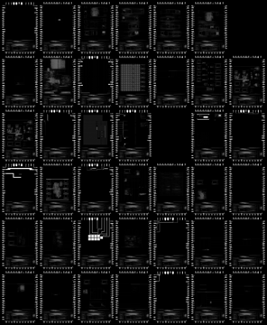
HVTRM
HLow VT PCh Radio* HVTRM = hvtr |
— | drawn 18:20 on mask GDS 98:0 |
0 of 40 unused on this shuttle |
0 |
 |
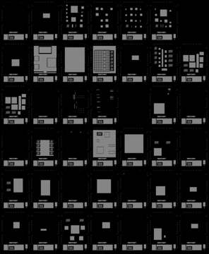
INDM
Inductor-TLM INDM = met3 (thick-last-metal flow, not SKY130) not used in SKY130 |
— | drawn 70:20 | 40 of 40 | 11,495,776 |
 |
NCM
N-Core Implant drawn ncm in the core plus a created periphery part like HVTPM; only the drawn part is rendered not used in SKY130 |
— | drawn 92:44 on mask GDS 17:0 derived 92:44 OR ((64:20 NOT 75:20) NOT 125:44) |
40 of 40 | 104,428 |
 |
RRM
RRAM mask the RRAM-stack mask (r1c) of the sky130B RRAM tier between met1 and met2. One drawn layer r1c = GDS 201/20 (open_pdks names it RERAM, short alias 'rr' -> 'rr' + M) defines all three physical films: rr1_bot_electrode, rr1_oxide, rr1_top_electrode. Only on the later sets 5CS8016AC/17AC/18AC. sky130A designs draw no 201/20, so those slots render empty sky130B RRAM tier (met1-met2); drawn layer r1c = GDS 201/20 not used in SKY130 |
— | drawn 201:20 | 0 of 40 unused on this shuttle |
0 |
 |
VIMC
Via 1 top, RRAM tier the second via1 mask of the sky130B RRAM tier (r1v). The RRAM splits via1 in two: the designer draws one 'via' shape, and mask generation separates it into via_bot (cviam = VIM) and via_top (r1v) wherever the via is enclosed by r1c. Rendered as via AND r1c. NOT CTM1/mcon, as once assumed: 8016/17/18 each carry a separate CTM1 plate (400), and 455 sits above MM1 (450) while mcon is below met1 sky130B RRAM tier; r1v, the upper half of the split via1 not used in SKY130 |
— | drawn 68:44 derived 68:44 AND 201:20 |
0 of 40 unused on this shuttle |
0 |
 |
VIPDM
Pad Via VIPDM = via3 (pad-via flow, not SKY130) not used in SKY130 |
— | drawn 70:44 | 40 of 40 | 34,408,584 |
These are renders of the drawn shapes that go on each photomask, taken from the layouts the shuttle's projects taped out — they are not photomask artwork: reticle pitch, the 4x reduction, mirroring and the frame features the fab adds are not modelled. An empty image is a real result; several mask layers are used by no project on a given shuttle. Each die's source layout is named in result.json and lives in the public shuttle repositories under foss-eda-tools.googlesource.com, so every image here can be traced back to the tape-out it came from. Generated with sky130-mask-decoder.